Tags
Language
Tags
April 2024
Su Mo Tu We Th Fr Sa
31 1 2 3 4 5 6
7 8 9 10 11 12 13
14 15 16 17 18 19 20
21 22 23 24 25 26 27
28 29 30 1 2 3 4
https://canv.ai/
The picture is generated by canv.ai

We are excited to announce that Canv.ai now features a built-in translator, allowing you to communicate in your native language. You can write prompts in your language, and they will be automatically translated into English, facilitating communication and the exchange of ideas!

We value freedom of speech and guarantee the absence of censorship on Canv.ai. At the same time, we hope and believe in the high moral standards of our users, which will help maintain a respectful and constructive atmosphere.


👉 Check for yourself!

Excitons in Low-Dimensional Semiconductors: Theory Numerical Methods Applications

Posted By: AvaxGenius
Excitons in Low-Dimensional Semiconductors: Theory Numerical Methods Applications

Excitons in Low-Dimensional Semiconductors: Theory Numerical Methods Applications by Stephan Glutsch
English | PDF | 2004 | 302 Pages | ISBN : 3540202404 | 24.8 MB

Low-dimensional semiconductors have become a vital part of today's semiconductor physics, and excitons in these systems are ideal objects that bring textbook quantum mechanics to life. Furthermore, their theoretical understanding is important for experiments and optoelectronic devices. The author develops the effective-mass theory of excitons in low-dimensional semiconductors and describes numerical methods for calculating the optical absorption including Coulomb interaction, geometry, and external fields. The theory is applied to Fano resonances in low-dimensional semiconductors and the Zener breakdown in superlattices. Comparing theoretical results with experiments, the book is essentially self-contained; it is a hands-on approach with detailed derivations, worked examples, illustrative figures, and computer programs. The book is clearly structured and will be valuable as an advanced-level self-study or course book for graduate students, lecturers, and researchers.

Fowler-Nordheim Field Emission: Effects in Semiconductor Nanostructures

Posted By: AvaxGenius
Fowler-Nordheim Field Emission: Effects in Semiconductor Nanostructures

Fowler-Nordheim Field Emission: Effects in Semiconductor Nanostructures by Sitangshu Bhattacharya , Kamakhya Prasad Ghatak
English | PDF (True) | 2012 | 353 Pages | ISBN : 3642204929 | 4.4 MB

This monograph solely presents the Fowler-Nordheim field emission (FNFE) from semiconductors and their nanostructures. The materials considered are quantum confined non-linear optical, III-V, II-VI, Ge, Te, carbon nanotubes, PtSb2, stressed materials, Bismuth, GaP, Gallium Antimonide, II-V, Bi2Te3, III-V, II-VI, IV-VI and HgTe/CdTe superlattices with graded interfaces and effective mass superlattices under magnetic quantization and quantum wires of the aforementioned superlattices. The FNFE in opto-electronic materials and their quantum confined counterparts is studied in the presence of light waves and intense electric fields on the basis of newly formulated electron dispersion laws that control the studies of such quantum effect devices. The importance of band gap measurements in opto-electronic materials in the presence of external fields is discussed from this perspective. This monograph contains 200 open research problems which form the very core and are useful for Ph. D students and researchers. The book can also serve as a basis for a graduate course on field emission from solids.

Nanowires and Nanobelts Materials, Properties and Devices. Volume 1: Metal and Semiconductor Nanowires

Posted By: AvaxGenius
Nanowires and Nanobelts Materials, Properties and Devices. Volume 1: Metal and Semiconductor Nanowires

Nanowires and Nanobelts Materials, Properties and Devices. Volume 1: Metal and Semiconductor Nanowires by Zhong Lin Wang
English | PDF | 2003 | 482 Pages | ISBN : 0387287051 | 54.1 MB

Volume 1, Metal and Semiconductor Nanowires covers a wide range of materials systems, from noble metals (such as Au, Ag, Cu), single element semiconductors (such as Si and Ge), compound semiconductors (such as InP, CdS and GaAs as well as heterostructures), nitrides (such as GaN and Si3N4) to carbides (such as SiC). The objective of this volume is to cover the synthesis, properties and device applications of nanowires based on metal and semiconductor materials. The volume starts with a review on novel electronic and optical nanodevices, nanosensors and logic circuits that have been built using individual nanowires as building blocks. Then, the theoretical background for electrical properties and mechanical properties of nanowires is given. The molecular nanowires, their quantized conductance, and metallic nanowires synthesized by chemical technique will be introduced next. Finally, the volume covers the synthesis and properties of semiconductor and nitrides nanowires.

Nanowires and Nanobelts: Materials, Properties and Devices

Posted By: AvaxGenius
Nanowires and Nanobelts: Materials, Properties and Devices

Nanowires and Nanobelts: Materials, Properties and Devices: Volume 2: Nanowires and Nanobelts of Functional Materials by Zhong Lin Wang
English | PDF (True) | 2003 | 304 Pages | ISBN : 038728706X | 21.5 MB

Volume 2, Nanowires and Nanobelts of Functional Materials covers a wide range of materials systems, from functional oxides (such as ZnO, SnO2, and In2O3), structural ceramics (such as MgO, SiO2 and Al2O3), composite materials (such as Si-Ge, SiC- SiO2), to polymers. This volume focuses on the synthesis, properties and applications of nanowires and nanobelts based on functional materials. Novel devices and applications made from functional oxide nanowires and nanobelts will be presented first, showing their unique properties and applications. The majority of the text will be devoted to the synthesis and properties of nanowires and nanobelts of functional oxides. Finally, sulphide nanowires, composite nanowires and polymer nanowires will be covered.

Lecture Notes on Principles of Plasma Processing

Posted By: AvaxGenius
Lecture Notes on Principles of Plasma Processing

Lecture Notes on Principles of Plasma Processing by Francis F. Chen , Jane P. Chang
English | PDF | 2003 | 213 Pages | ISBN : 0306474972 | 26.1 MB

Plasma processing of semiconductors is an interdisciplinary field requiring knowledge of both plasma physics and chemical engineering. The two authors are experts in each of these fields, and their collaboration results in the merging of these fields with a common terminology. Basic plasma concepts are introduced painlessly to those who have studied undergraduate electromagnetics but have had no previous exposure to plasmas. Unnecessarily detailed derivations are omitted; yet the reader is led to understand in some depth those concepts, such as the structure of sheaths, that are important in the design and operation of plasma processing reactors. Physicists not accustomed to low-temperature plasmas are introduced to chemical kinetics, surface science, and molecular spectroscopy. The material has been condensed to suit a nine-week graduate course, but it is sufficient to bring the reader up to date on current problems such as copper interconnects, low-k and high-k dielectrics, and oxide damage. Students will appreciate the web-style layout with ample color illustrations opposite the text, with ample room for notes.

Fundamentals of Inelastic Electron Scattering

Posted By: AvaxGenius
Fundamentals of Inelastic Electron Scattering

Fundamentals of Inelastic Electron Scattering by Peter Schattschneider
English | PDF | 1986 | 205 Pages | ISBN : 3211819371 | 14.2 MB

Electron energy loss spectroscopy (ELS) is a vast subject with a long and honorable history. The problem of stopping power for high energy particles interested the earliest pioneers of quantum mechanics such as Bohr and Bethe, who laid the theoretical foun­ dations of the subject. The experimental origins might perhaps be traced to the original Franck-Hertz experiment. The modern field includes topics as diverse as low energy reflection electron energy loss studies of surface vibrational modes, the spectroscopy of gases and the modern theory of plasmon excitation in crystals. For the study of ELS in electron microscopy, several historically distinct areas of physics are relevant, including the theory of the Debye­ Waller factor for virtual inelastic scattering, the use of complex optical potentials, lattice dynamics for crystalline specimens and the theory of atomic ionisation for isolated atoms. However the field of electron energy loss spectroscopy contains few useful texts which can be recommended for students. With the recent appearance of Raether's and Egerton's hooks (see text for references), we have for the first time both a comprehensive review text-due to Raether-and a lucid introductory text which emphasizes experimental aspects-due to Egerton. Raether's text tends to emphasize the recent work on surface plasmons, while the strength of Egerton's book is its treatment of inner shell excitations for microanalysis, based on the use of atomic wavefunctions for crystal electrons.

Fault-Tolerance Techniques for SRAM-Based FPGAs (Repost)

Posted By: AvaxGenius
Fault-Tolerance Techniques for SRAM-Based FPGAs (Repost)

Fault-Tolerance Techniques for SRAM-Based FPGAs by Fernanda Lima Kastensmidt , Luigi Carro , Ricardo Reis
English | PDF | 2006 | 193 Pages | ISBN : 0387310681 | 6.1 MB

Fault-tolerance in integrated circuits is not an exclusive concern regarding space designers or highly-reliable application engineers. Rather, designers of next generation products must cope with reduced margin noises due to technological advances. The continuous evolution of the fabrication technology process of semiconductor components, in terms of transistor geometry shrinking, power supply, speed, and logic density, has significantly reduced the reliability of very deep submicron integrated circuits, in face of the various internal and external sources of noise. The very popular Field Programmable Gate Arrays, customizable by SRAM cells, are a consequence of the integrated circuit evolution with millions of memory cells to implement the logic, embedded memories, routing, and more recently with embedded microprocessors cores.

Lectures on Non-linear Plasma Kinetics

Posted By: AvaxGenius
Lectures on Non-linear Plasma Kinetics

Lectures on Non-linear Plasma Kinetics by Vadim N. Tsytovich
English | PDF | 1995 | 380 Pages | ISBN : 3642789048 | 34.8 MB

Lectures on Non-linear Plasma Kinetics is an introduction to modern non-linear plasma physics showing how many of the techniques of modern non-linear physics find applications in plasma physics and how, in turn, the results of this research find applications in astrophysics. Emphasis is given to explaining the physics of nonlinear processes and the radical change of cross-sections by collective effects. The author discusses new nonlinear phenomena involving the excitation of coherent nonlinear structures and the dynamics of their random motions in relation to new self-organization processes. He also gives a detailed description of applications of the general theory to various research fields, including the interaction of powerful radiation with matter, controlled thermonuclear research, etc.

Electrical Characterization of Silicon-on-Insulator Materials and Devices

Posted By: AvaxGenius
Electrical Characterization of Silicon-on-Insulator Materials and Devices

Electrical Characterization of Silicon-on-Insulator Materials and Devices by Sorin Cristoloveanu , Sheng S. Li
English | PDF | 1995 | 389 Pages | ISBN : 0792395484 | 35.5 MB

Silicon on Insulator is more than a technology, more than a job, and more than a venture in microelectronics; it is something different and refreshing in device physics. This book recalls the activity and enthu­ siasm of our SOl groups. Many contributing students have since then disappeared from the SOl horizon. Some of them believed that SOl was the great love of their scientific lives; others just considered SOl as a fantastic LEGO game for adults. We thank them all for kindly letting us imagine that we were guiding them. This book was very necessary to many people. SOl engineers will certainly be happy: indeed, if the performance of their SOl components is not always outstanding, they can now safely incriminate the relations given in the book rather than their process. Martine, Gunter, and Y. S. Chang can contemplate at last the amount of work they did with the figures.

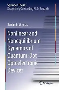
Nonlinear and Nonequilibrium Dynamics of Quantum-Dot Optoelectronic Devices

Posted By: AvaxGenius
Nonlinear and Nonequilibrium Dynamics of Quantum-Dot Optoelectronic Devices

Nonlinear and Nonequilibrium Dynamics of Quantum-Dot Optoelectronic Devices by Benjamin Lingnau
English | PDF (True) | 2015 | 203 Pages | ISBN : 3319258036 | 7.9 MB

This thesis sheds light on the unique dynamics of optoelectronic devices based on semiconductor quantum-dots. The complex scattering processes involved in filling the optically active quantum-dot states and the presence of charge-carrier nonequilibrium conditions are identified as sources for the distinct dynamical behavior of quantum-dot based devices. Comprehensive theoretical models, which allow for an accurate description of such devices, are presented and applied to recent experimental observations. The low sensitivity of quantum-dot lasers to optical perturbations is directly attributed to their unique charge-carrier dynamics and amplitude-phase-coupling, which is found not to be accurately described by conventional approaches. The potential of quantum-dot semiconductor optical amplifiers for novel applications such as simultaneous multi-state amplification, ultra-wide wavelength conversion, and coherent pulse shaping is investigated. The scattering mechanisms and the unique electronic structure of semiconductor quantum-dots are found to make such devices prime candidates for the implementation of next-generation optoelectronic applications, which could significantly simplify optical telecommunication networks and open up novel high-speed data transmission schemes.

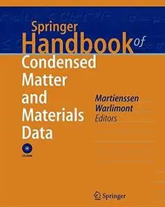
Springer Handbook of Condensed Matter and Materials Data

Posted By: AvaxGenius
Springer Handbook of Condensed Matter and Materials Data

Springer Handbook of Condensed Matter and Materials Data by Werner Martienssen, Hans Warlimont
English | PDF (True) | 2005 | 1121 Pages | ISBN : 3540443762 | 37.3 MB

Springer Handbook of Condensed Matter and Materials Data provides a concise compilation of data and functional relationships from the fields of solid-state physics and materials in this 1200 page volume. The data, encapsulated in 914 tables and 1025 illustrations, have been selected and extracted primarily from the extensive high-quality data collection Landolt-Börnstein and also from other systematic data sources and recent publications of physical and technical property data. Many chapters are authored by Landolt-Börnstein editors, including the prominent Springer Handbook editors, W. Martienssen and H. Warlimont themselves.

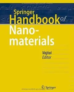
Springer Handbook of Nanomaterials (Repost)

Posted By: AvaxGenius
Springer Handbook of Nanomaterials (Repost)

Springer Handbook of Nanomaterials by Robert Vajtai
English | PDF (True) | 2013 | 1234 Pages | ISBN : 3642205941 | 102.1 MB

The Springer Handbook of Nanomaterials covers the description of materials which have dimension on the "nanoscale". The description of the nanomaterials in this Handbook follows the thorough but concise explanation of the synergy of structure, properties, processing and applications of the given material. The Handbook mainly describes materials in their solid phase; exceptions might be e.g. small sized liquid aerosols or gas bubbles in liquids. The materials are organized by their dimensionality. Zero dimensional structures collect clusters, nanoparticles and quantum dots, one dimensional are nanowires and nanotubes, while two dimensional are represented by thin films and surfaces. The chapters in these larger topics are written on a specific materials and dimensionality combination, e.g. ceramic nanowires. Chapters are authored by well-established and well-known scientists of the particular field. They have measurable part of publications and an important role in establishing new knowledge of the particular field.

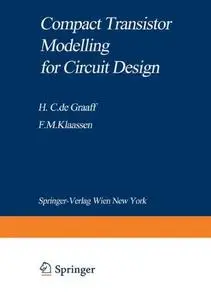
Compact Transistor Modelling for Circuit Design

Posted By: AvaxGenius
Compact Transistor Modelling for Circuit Design

Compact Transistor Modelling for Circuit Design by Henk C. Graaff , François M. Klaassen
English | PDF | 1990 | 366 Pages | ISBN : 3709190452 | 26.5 MB

During the first decade following the invention of the transistor, progress in semiconductor device technology advanced rapidly due to an effective synergy of technological discoveries and physical understanding. Through physical reasoning, a feeling for the right assumption and the correct interpretation of experimental findings, a small group of pioneers conceived the major analytic design equations, which are currently to be found in numerous textbooks. Naturally with the growth of specific applications, the description of some characteristic properties became more complicated. For instance, in inte­ grated circuits this was due in part to the use of a wider bias range, the addition of inherent parasitic elements and the occurrence of multi­ dimensional effects in smaller devices. Since powerful computing aids became available at the same time, complicated situations in complex configurations could be analyzed by useful numerical techniques. Despite the resulting progress in device optimization, the above approach fails to provide a required compact set of device design and process control rules and a compact circuit model for the analysis of large-scale electronic designs. This book therefore takes up the original thread to some extent. Taking into account new physical effects and introducing useful but correct simplifying assumptions, the previous concepts of analytic device models have been extended to describe the characteristics of modern integrated circuit devices. This has been made possible by making extensive use of exact numerical results to gain insight into complicated situations of transistor operation.

GaAs Devices and Circuits

Posted By: AvaxGenius
GaAs Devices and Circuits

GaAs Devices and Circuits by Michael Shur
English | PDF | 1987 | 677 Pages | ISBN : 0306421925 | 50.1 MB

GaAs devices and integrated circuits have emerged as leading contenders for ultra-high-speed applications. This book is intended to be a reference for a rapidly growing GaAs community of researchers and graduate students. It was written over several years and parts of it were used for courses on GaAs devices and integrated circuits and on heterojunction GaAs devices developed and taught at the University of Minnesota. Many people helped me in writing this book. I would like to express my deep gratitude to Professor Lester Eastman of Cornell University, whose ideas and thoughts inspired me and helped to determine the direction of my research work for many years. I also benefited from numerous discussions with his students and associates and from the very atmosphere of the pursuit of excellence which exists in his group.

Two-Dimensional Superconductivity in Rare Earth Oxybismuthides with Unusual Valent Bismuth Square Net

Posted By: AvaxGenius
Two-Dimensional Superconductivity in Rare Earth Oxybismuthides with Unusual Valent Bismuth Square Net

Two-Dimensional Superconductivity in Rare Earth Oxybismuthides with Unusual Valent Bismuth Square Net by Ryosuke Sei
English | PDF EPUB (True) | 2023 (2024 Edition) | 124 Pages | ISBN : 9819973120 | 44.6 MB

This book elucidates fascinating electronic phenomena of unusual Bi2-square net in layered R2O2Bi (R: rare earth) compounds using two approaches: the fabrication of epitaxial thin films and the synthesis of bulk polycrystalline powders. The Bi2-square net compounds are a promising platform to explore exotic physical properties originating from the interplay between a two-dimensional electronic state and strong spin–orbit coupling; however, there are few reports on Bi2-square net compounds due to the instability of unusual electronic configurations.